 www.LED
 SEMICONDUCTOR
Our German sites are much more detailed then our English sites. So please switch in our Germen sites and use the language translater (top right) with 60 languages.
Semiconductors are divided in two groups: Into direct and into indirect semiconductors. The difference exists in the tape structure of the impulse area. For LEDs only direct semiconductors can be used. This is because of the fact that with direct semiconductor both band edges (valence band and the next higher conduction band) exhibit an extremum nearly with the same quasi-impulse lie. Here photons can be delivered now with recombination by electron hole pairs. With indirect semiconductor is appropriate that for extrema with different quasi-impulses and the energy as warmth (lattice vibration) is delivered. More under Wikipedia.
In this chapter we try to dig ia little bit more into the semiconductor thematic with a few fundamental information:
The atoms regularly arranged in the crystal lattice do not rest motionlessly on their lattice sites, but they swing, or better described, they vibrate around their middle positions. With rising temperature these oscillations becomes stronger.
The middle oscillation energy is proportional to the temperature and amounts to at room temperature approximately 0.025 eV.
Many atoms have a smaller energy, some a higher and only very few atoms an energy, which is sufficient, in order to drive an electron out from its connection (bond energy).
These electrons are available then as freely mobile conduction electrons and can follow an electrical field. (also by incident light radiation the necessary energy can be supplied, this e.g. is used with the solar cell.)
For simple comprehensibility we try to imagine now the following:
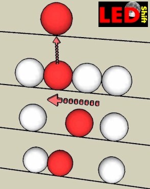
 Beside our bowling rink lies the Bowling channel, in which the balls are "parked" and wait for our throw. The channel is full and there is no space that a bowling ball can be shifted ore addited. The separation of an electron (in our case the ball) from the connection to lattice atoms (all balls in the groove) can be compared then with the following procedure:
In order to be able to play with any ball to make mobile i.e. her one must lift it out with effort of force (bond energy) from the ball federation.
By individual catching up of the other balls thus the gap moves against the balls.
Only which role now plays the positive ions, which remain after release of an electron stationarily bound to their lattice site?
Since an electron is missing to them, now one speaks of a "mobile hole", or "electron hole".
Everyone of these positive ions can "drop out" an electron from a lying close lattice atom and become neutral again. With "robbed" lattice atom develops thereby again an electron hole. In an outside field the electron hole moves like a positive charge, but not by slipping of the rail of the ions, but as described above as, by re squeezing of the electrons. Thus the electron holes contribute to the charge transfer.
If a conduction electron comes now too close to an electron hole the positive charge binds the electron and it "falls" into the hole, which both charge carriers neutralize themselves and they
The conductivity of a pure semiconductor crystal is based on the formation of freely mobile charge carriers:
Electrons and electron holes.
The electron holes behave like positive charges. The conductivity increases with rising temperature.
The doped semiconductor
The doped semiconductor in a pure semiconductor crystal are always exactly equivalent conduction electrons as electron holes. The number of the freely mobile charge carriers and thus the conductivity of a semiconductor can be considerably increased by the addition of certain foreign atoms. We speak then of ad o p e d semiconductors
Electron excess conductor (n-conductor)
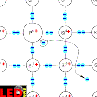
 We imagine that a small part of the SI atoms in the crystal by foreign atoms of the 5. Main group, e.g. phosphorus atoms, to be exchanged. More usually point one from 10h4 to 10h7 siliciumatomen in the crystal lattice is replaced by one phosphorus atom. Phosphorus possesses five electrons in the external electron sheath however, from which only four at the connection with the adjacent siliciumatomen can participate.
The fifth electron is bound not to the crystal lattice and can easily be separated by the phosphorus atom. The immovable Phosphor ion staying is thus positively charged.
Since it delivered an electron now, this semiconductor is called contributor or D o n a t o r .
The necessary energy for this separation is substantially smaller than the middle oscillation energy of the crystal lattice atoms. Even already at room temperature almost all phosphorus atoms lose their fifth electron by these "thermal shocks". If one produces now e.g. a concentration of a phosphorus atom on 10h6 siliciumatomen, this means that with a density of for instance 10h22 atoms per cm³, a density of 10h16 per cm³ at free moving electrons exists. Pure silicon contains for instanceH.R.H.0 free electrons per cm³. This confirms clearly the substantially higher conductivity of the doped semiconductor.
This doping with pentavalent atoms leads thus to increase of free moving electrons and to the increased conductivity opposite to pure semiconductors. One speaks therefore of an electron excess conductor or a n-conductor. The, however in the semiconductor always existing, equal free electrons and electron holes contribute only few to the conductivity.
Electron deficiency conductor (p-conductor)
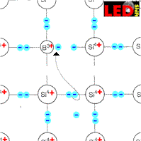
 If we insert however now only trivalent e.g. boron atoms into a Siliciumcristal, then this electron is missing to the boron atoms, in order to manage the connections to all four silicon neighbors by pairs of electrons.
But from where can this missing electron be robbed?
Naturally of the adjacent siliciumatomes and thus is missing again this robbed atom electrons and we recognize that additional electron holes were produced as charge carriers.
Boron atoms, which caught an electron, are called A k z e p t o r e n.
They are negatively charged and to their lattice sites bound. The electron holes produced by them stand thus for the charge transfer for order and their density are determined by the density of the acceptor atoms . It exceeds the density of the free moving electrons around a multiple. When putting on a current the electron holes behave like positive charge carriers. We call it therefore electron deficiency conductor or p-conductor.
| AGB Ledshift | LED Function | LED Producer | LED Distributor | LED Events | LED Company Entry | LEDS | Sitemap | Contact | |
|
|
© Markus Kottas, Heldenberg Ltd.2018